sup dawg heard you’d like to machine things at MIT, here’s what’s up:
Step 1: Get inside the TARDIS
 |
| source |
Step 2: Arrive in China
 |
Step 3: Make friends in China and tour factories
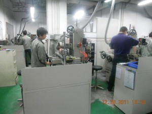 |
Okay I lie. this is actually a machine shop and not a factory, but here be precision prototypes ala Charles’s outsourced hubmotor casings made
Also, protip: if you ever do visit a factory, don’t be like me and pretend to be a factory worker and **** up all the parts while working 5x slower than everyone else >__<;;;
Step 5: profit!!!11!!
…
… …
Ehem.
Oh right. Sorry. I’m supposed to not fail 2.671 and graduate so I will start on MIT machine shops now. First, I’ll overview the generally accessible shops, then I’ll go over waterjet / lasercutter access. In particular, I will address this as a major-neutral FAQ instead of a pictorial / virtual tour of machine shops around campus.
Q: How do I learn to machine?
A1: Edgerton shop training.
Sign up for the Edgerton shop training waiting list right now. Seriously, right NOW. All you have to do is send a measly email and it takes upwards of a semester to get off the waiting list.
“The monthly training program is conducted in the evenings and consists of twelve hours of hands on instruction, showing the basics of milling and lathe work by making two small parts”
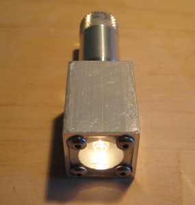
At the end you even get to take home this beauty which you created from stock rod and bar:
 |
| source |
It’s also IMHO much more actually useful than your two weeks of 2.670 (which are more like “heyyy guys check out these tools at your disposal, j/k we set them up for you) or even 2.007 and 2.008 if you don’t take the initiative and swim counter-current, the shop guys (bless their hearts) will do a lot of the setup work for you in order to keep the class running smoothly (esp. toward the end of semester, when you know what you want to do but so does everyone else).
When I took 2.007 I contemplated taking advantage of my free time / their free time early in the semester, but was told they wouldn’t tolerate non-class projects “just to learn machining.” I now think that’s false, but it’s still nerve-wracking for someone like me to just go up to them, esp. since at the time I didn’t know what sort of beginner level projects I could try out just for fun, so I just ended up skulking around MITERS.
A2: Take “How to Make (Almost) Anything“.
This is much more of a crapshoot, as it’s offered only 1x a year to 40 people (usu ~150 people apply). However, they actively try to create a “class” of different background each year: undergrads, grads, architecture, media lab, no “making” experience, machining experts, all have a chance of getting in.
For reference, this is the prof on CNN and at TEDtalks, and this is the class website as well as the subject listing.
Q: What shops are open to me to work on personal projects as an undergrad?
A: Hobby Shop, Edgerton, MITERS.
It’s also an open secret that you can judiciously use your UROP shop access for personal projects; see later in this post for more info on UROP shops (the biggest ones are Media Lab’s and CSAIL’s). In addition, several dorms / some students have their own mini-machine shops.
- Edgerton
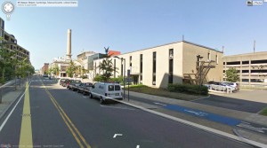
It’s right behind CSAIL. Entrance is to the right, under the external staircase. - Who it’s open to:
- “The Edgerton Center Student Shop provides training in the use of machine tools, access to them, and guidance in project planning, to any current MIT student.”
- Types of Projects:
- “Once you’ve completed the course, you’re free to use the shop whenever you want, whether it’s for a class project, a student group you’re working with, or your own fun idea” (src)
- Safety:
- Either take the shop training class or test out of it and just take an hour-ish edgerton shop familiarization lecture
- Hours:
- Open “business hours”, aka “9 to 5”-ish.
- Cost:
- Free
- Noteworthy Equipment:
- CNC mills and lathe
- welding (mig, tig, stick)
- Sometimes staffed by students
- Hobby Shop
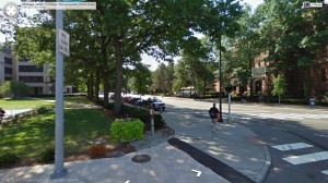
Almost next door to the student center. Entrance 1: door under white box (right part of image) 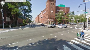
Entrance 2: door under white box (left part of image) - Who it’s open to:
- “Membership to the Hobby Shop is open to MIT students, staff, faculty, retirees, alumni/ae, and their spouses”
- “Today, the Hobby Shop provides a place for any MIT student, regardless of major or experience, to work with a wide range of well maintained machines and tools and to receive instruction, as well as practical design and building advice.
- “The Hobby Shop now offers its own classes” (mostly IAP ones around specific projects, I think)
- Types of Projects:
- “Projects can be academic or personal, serious or just for fun.” (src)
- Safety:
- Don’t really need machining experience (the instructors will help you when you have your project in mind), take the shop orientation and you’re set
- Hours:
- B
- Business hours
- Cost:
- $30 / term (spring, summer, fall) or $75 / year
- Noteworthy Equipment:
- More woodworking tools than anywhere else
- CNC mill and lathe
- Waterjet (membership + $2/minute)
- Equipment List (with pictures even! very nicely done)
- MITERS
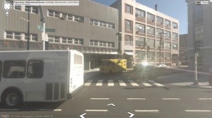
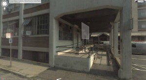
Same building complex as MIT Museum (across from Random / Shaw’s). Entrance 1: under white box (to left of yellow truck) - Who it’s open to:
- “We are a student group promoting making things for the fun it. We are MIT’s only student-run shop, and we do not receive funding from any MIT department.” (src)
- Open to everyone, but especially MIT undergrads
- Types of Projects:
- “It’s a member-run creative haven and build-anything-you-want, if-you-break-it,-fix-it space.” (src)
- Class projects, UROPs, and projects-just-for-fun all welcome, as long as you contribute back by keeping the shop clean and hanging out with us
- Safety:
- Edgerton shop training highly recommended
- Only open when a keyholder (student who’s hung out a lot, i.e. know the quirks of MITERS’s equipment, and has taken Edgerton training) is there
- Hours:
- Whenever a keyholder is there, aka almost 24/7. Once you become a keyholder yourself, you can go whenever you want (though if you’re working w/ power tools, must have at least one other person with you).
- When I took 6.131, lab closed at midnight and we’d all migrate to MITERS to pull an all-nighter
- Cost:
- Noteworthy Equipment:
- EE lab as well — components, power supplies, oscilloscopes, pcb etching
- welding a possibility, email our list directly for more details
- Manual lathe, numeric read-out (not CNC) mill
- Equipment List (with pics)
~~~following WIP, to be fleshed out~~~
Waterjet: media lab (24/7), CSAIL (24/7), architecture bldg10 4th floor (24/7 I think), 2.007, hobby shop … idk other shops (16?)
- UROP or take classes @ media lab and sign up for their shop training right away (24/7 access)
- UROP @ CSAIL and sign up for shop training right away (24/7 access)
- course 4 major
Lasercutter: media lab (24/7), CSAIL (24/7), architecture (24/7), 2.007?, commercial shop by 2 MIT alumni: danger!awesome right near Central T stop / Toscii’s, … idk other shops (16?)
- urop / class @ media lab
- urop @ csail
- csail
- be course 4 major
Injection molding: yea right. take 2.008 and make friends with the shop guys?
Vacuum forming: media lab (24/7), architecture (24/7), 2.008
small CNC mill, milling / etching: roll your own for ~$200 with waterjet and scrap Al
Stock: MIT central machine shop, McMaster-Carr, Turner Steel
ee-ish: hobbyking, ebay, amazon surprisingly
silicon molds / plastic / food-safe: smooth-on
through ECAT vendor for your UROP: digikey, mouser, jameco
~~~~~~
Appendix, LMP
The Manufacturing Lab in building 35 will be open for extended hours on Tuesday’s & Thursday’s from 5 – 8 PM for use as a trial period under the following criteria starting next Tuesday 2/28/12:
- Students will need to meet with the technical instructor prior to starting any work and sign in & out on the evening sign in sheet.
- There will be a maximum of 8 students allowed in the shop.
- This time is for Mech E students only
- Graduate Research and SB Thesis; UROP; and personal projects can be done during this time with priorities in that order.
- No course work can be done during this time.
- This time cannot be used for any non-MIT project, or for extramural consulting work.
- Not all machinery will be available for use (IE: waterjet, injection molder, 5 axis mill).
- Students are required to supply their own raw materials.
- You can reserve a spot in advance by emailing bbuckley@mit.edu
- Should you not show for a reserved spot you will not be able to reserve a spot in the future.
- We will not be able to support and teams or clubs during this trial period but may be reviewed in the future.
Mary Boyce, John Lienhard and Bill Buckley
~~~~~~
Appendix, online resources
no substitute for learning in person!
http://www.machinistblog.com/mit-techtv-machine-shop-videos/
http://electron.mit.edu/~gsteele/mirrors/www.nmis.org/EducationTraining/machineshop/outline.html
~~~~~~
Conclusion
 |
| ^___^ |

![how do I machine shop [at MIT]?](https://orangenarwhals.com/wp-content/uploads/2012/03/tardis2-550x372.jpg)
